- 您现在的位置:买卖IC网 > Sheet目录872 > P036T048T12AL (Vicor Corporation)V.I CHIP PRM REGULATOR 48V 120W
�� �
�
�Pin� /� Control� Functions�
�+In� /� -In� DC� Voltage� Ports�
�V?I� Chip� Regulator�
�The� V?I� Chip� maximum� input� voltage� should� not� be� exceeded.� PRMs�
�have� internal� over� /� undervoltage� lockout� functions� that� prevent�
�operation� outside� of� the� specified� input� range.� PRMs� will� turn� on� when�
�the� input� voltage� rises� above� its� undervoltage� lockout.� If� the� input�
�voltage� exceeds� the� overvoltage� lockout,� PRMs� will� shut� down� until� the�
�AL� Version�
�VH�
�SC�
�SG�
�OS�
�NC�
�CD�
�A�
�B�
�C�
�D�
�E�
�F�
�4�
�3�
�2�
�1�
�A�
�B�
�C�
�D�
�E�
�F�
�VC�
�PC�
�TM�
�IL�
�NC�
�PR�
�overvoltage� fault� clears.� PC� will� toggle� indicating� an� out� of� bounds�
�G�
�G�
�condition.�
�+OUT�
�H�
�J�
�H�
�J�
�+IN�
�K�
�K�
�+Out� /� -Out� Factorized� Voltage� Output� Ports�
�These� ports� provide� the� Factorized� Bus� voltage� output.� The� –Out� port� is�
�–OUT�
�L�
�M�
�N�
�P�
�L�
�M�
�N�
�P�
�–IN�
�connected� internally� to� the� –In� port� through� a� current� sense� resistor.�
�The� PRM� has� a� maximum� power� and� a� maximum� current� rating� and� is�
�Bottom� View�
�protected� if� either� rating� is� exceeded.� Do� not� short� –Out� to� –In.�
�VC� –� VTM� Control�
�The� VTM� Control� (VC)� port� supplies� an� initial� V� CC� voltage� to�
�downstream� VTMs,� enabling� the� VTMs� and� synchronizing� the� rise� of�
�the� VTM� output� voltage� to� that� of� the� PRM.� The� VC� port� also� provides�
�feedback� to� the� PRM� to� compensate� for� voltage� drop� due� to� the� VTM�
�output� resistance.� The� PRM’s� VC� port� should� be� connected� to� the� VTM�
�VC� port.� A� PRM� VC� port� can� drive� a� maximum� of� two� (2)� VTM� VC� ports.�
�PC� –� Primary� Control�
�The� PRM� voltage� output� is� enabled� when� the� PC� pin� is� open� circuit�
�(floating).� To� disable� the� PRM� output� voltage,� the� PC� pin� is� pulled� low.�
�Open� collector� optocouplers,� transistors,� or� relays� can� be� used� to�
�Signal� Name�
�+In�
�–In�
�VC�
�PC�
�TM�
�IL�
�PR�
�VH�
�SC�
�SG�
�OS�
�CD�
�+Out�
�–Out�
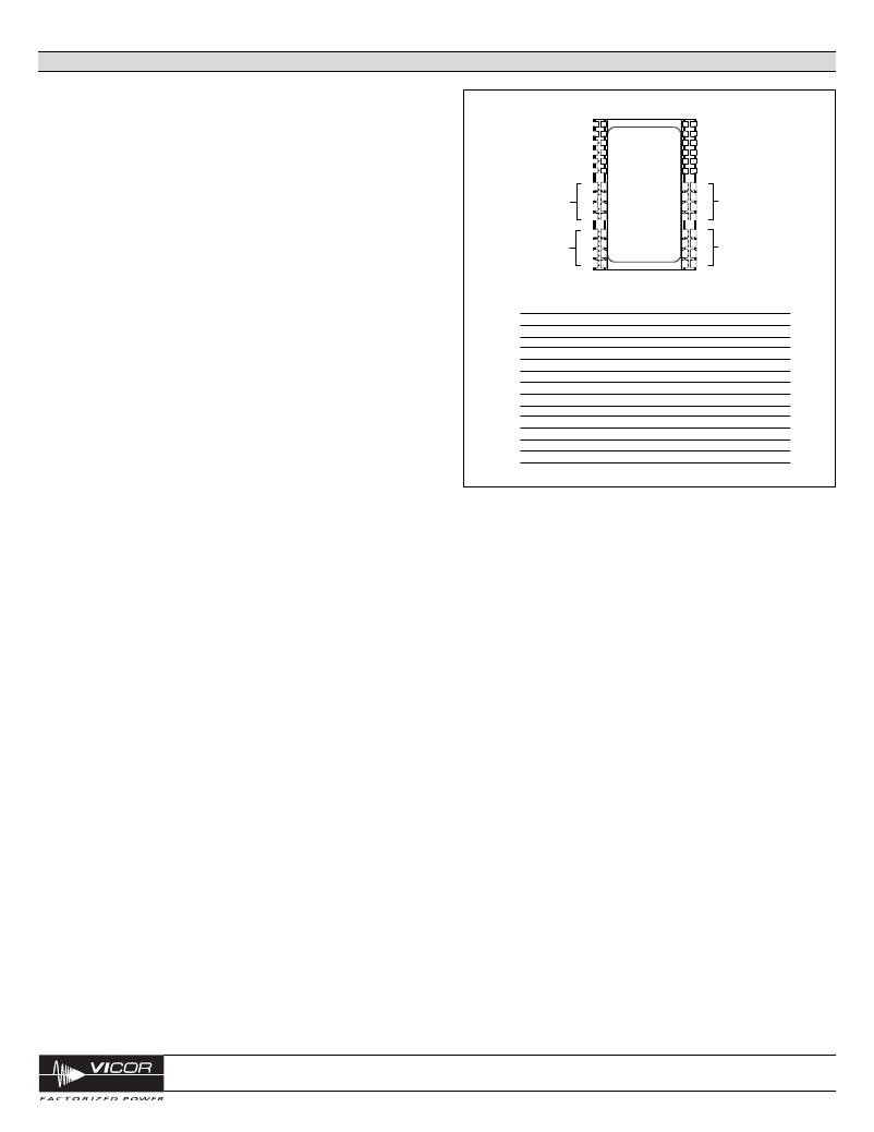
�Figure� 15� —� PRM� pin� configuration�
�Designation�
�G1-K1,G2-K2�
�L1-P1,� L2-P2�
�A1,A2�
�B1,� B2�
�C1,� C2�
�D1,� D2�
�F1,� F2�
�A3,� A4�
�B3,� B4�
�C3,� C4�
�D3,� D4�
�F3,� F4�
�G3-K3,� G4-K4�
�L3-P3,� L4-P4�
�control� the� PC� pin.� When� using� multiple� PRMs� in� a� high� power� array,�
�the� PC� ports� should� be� tied� together� to� synchronize� their� turn� on.�
�During� an� abnormal� condition� the� PC� pin� will� pulse� (Fig.12)� as� the� PRM�
�initiates� a� restart� cycle.� This� will� continue� until� the� abnormal� condition�
�is� rectified.� The� PC� should� not� be� used� as� an� auxiliary� voltage� supply,�
�nor� should� it� be� switched� at� a� rate� greater� than� 1� Hz.�
�TM� –� Factory� Use� Only�
�SC� –� Secondary� Control�
�The� load� voltage� may� be� controlled� by� connecting� a� resistor� or� voltage�
�source� to� the� SC� port.� The� slew� rate� of� the� output� voltage� may� be�
�controlled� by� controlling� the� rate-of-rise� of� the� voltage� at� the� SC� port�
�(e.g.,� to� limit� inrush� current� into� a� capacitive� load).�
�SG� –� Signal� Ground�
�This� port� provides� a� low� inductance� Kelvin� connection� to� –In� and�
�should� be� used� as� reference� for� the� OS,� CD,� SC,VH� and� IL� ports.�
�IL� –� Current� Limit� Adjust�
�The� PRM� has� a� preset,� maximum,� current� limit� set� point.� The� IL� port�
�may� be� used� to� reduce� the� current� limit� set� point� to� a� lower� value.� See�
�“adjusting� current� limit”� on� page� 10.�
�PR� –� Parallel� Port�
�The� PR� port� signal,� which� is� proportional� to� the� PRM� output� power,�
�supports� current� sharing� of� two� PRMs.� To� enable� current� sharing,� PR�
�ports� should� be� interconnected.� Steps� should� be� taken� to� minimize�
�coupling� noise� into� the� interconnecting� bus.� Terminate� this� port� with� a�
�10� k� equivalent� resistance� to� SG,� e.g.� 10� k� for� a� single� PRM,� 20� k� each�
�for� 2� PRMs� in� parallel,� 30� k� each� for� 3� PRMs� in� parallel� etc..� Please�
�consult� Vicor� Applications� Engineering� regarding� additional�
�considerations� when� paralleling� more� than� two� PRMs.�
�VH� –� Auxiliary� Voltage�
�VH� is� a� gated� (e.g.� mirrors� PC),� non-isolated,� nominally� 9� Volt,�
�regulated� DC� voltage� (see� “Auxiliary� Pins”� specifications,� on� Page� 7)�
�that� is� referenced� to� SG.� VH� may� be� used� to� power� external� circuitry�
�having� a� total� current� consumption� of� no� more� than� 5� mA� under� either�
�transient� or� steady� state� conditions� including� turn-on.�
�OS� –� Output� Set�
�The� application-specific� value� of� the� Factorized� Bus� voltage� (Vf)� is� set�
�by� connecting� a� resistor� between� OS� and� SG.� Resistor� value� selection� is�
�shown� in� Table� 1� on� Page� 2,� and� described� on� Page� 9.� If� no� resistor� is�
�connected,� the� PRM� output� will� be� approximately� one� volt.� If� set�
�resistor� is� not� collocated� with� the� PRM� a� load� bypass� capacitor� of�
�~200� pF� may� be� required.�
�CD� –� Compensation� Device�
�Adaptive� Loop� control� is� configured� by� connecting� an� external� resistor�
�between� the� CD� port� and� SG.� Selection� of� an� appropriate� resistor� value�
�(see� Equation� 2� on� Page� 9� and� Table� 1� on� Page� 2)� configures� the� PRM�
�to� compensate� for� voltage� drops� in� the� equivalent� output� resistance� of�
�the� VTM� and� the� PRM-VTM� distribution� bus.� If� no� resistor� is� connected�
�to� CD,� the� PRM� will� be� in� Local� Loop� mode� and� will� regulate� the�
�+Out� /� –Out� voltage� to� a� fixed� value.�
�vicorpower.com�
�800-735-6200�
�V?I� Chip� Regulator�
�P036F048T12AL�
�Rev.� 1.9�
�Page� 8� of� 14�
�发布紧急采购,3分钟左右您将得到回复。
相关PDF资料
P045T048T17AL
V.I CHIP PRM REGULATOR 48V 170W
P045T048T32AL
V.I CHIP PRM REGULATOR 48V 320W
P048T048M24AL
V.I CHIP PRM REGULATOR 48V 240W
P048T048T12AL
V.I CHIP PRM REGULATOR 48V 120W
P081N-271F2CBR10K
POT MODULE 8MM 10K SIDE ADJ
P090L-02T20BR50K
POT ROTARY 50K OHM 9MM SNAPIN
P092N-QC15AR20K
POT ROTARY 20K OHM 9MM
P110KH1-0F25BR10K
POT ROTARY 10K OHM 11MM BUSHING
相关代理商/技术参数
P037253-001
制造商:Superior Electric 功能描述:Auxiliary Equipment - T5587* Paralleling Choke Cpver
P037S
制造商:Pro-Signal 功能描述:TRANSFORMER AUDIO 100V LINE 4W 制造商:PRO SIGNAL 功能描述:TRANSFORMER, AUDIO, 100V LINE, 4W
P037T
制造商:Pro-Signal 功能描述:TRANSFORMER AUDIO 100V LINE 8W 制造商:PRO SIGNAL 功能描述:TRANSFORMER, AUDIO, 100V LINE, 8W
P037U
制造商:Pro-Signal 功能描述:TRANSFORMER AUDIO 100V LINE 16W
P038
制造商:未知厂家 制造商全称:未知厂家 功能描述:TRANSISTOR | BJT | PNP | 300V V(BR)CEO | 500MA I(C) | TO-92
P038
制造商:Pro-Signal 功能描述:TRANSFORMER AUDIO 100V LINE 15W
P0380
制造商:TE Connectivity 功能描述:
P-038347-0082
制造商:Edwards Signaling & Security Systems 功能描述:HORN ASM ATLAS 30W